
Home|Research|People|Publication|Facility|Contact|日本語HP
Thin Film Deposition Equipments:
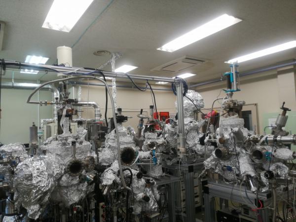 |
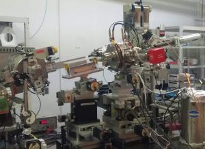
This UHV cluster is mainly used for basic material research. Key features:
|
| UHV Cluster No. 1 | |
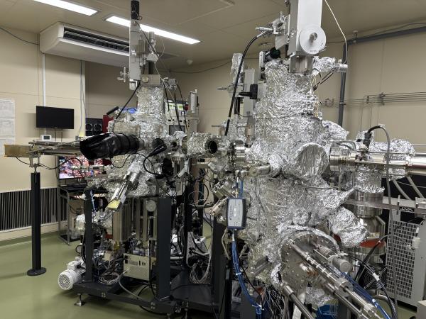 |
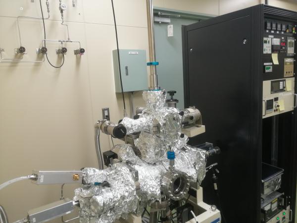
This UHV cluster is mainly used for device (such as MRAM) development. Key features:
|
| UHV Cluster No.2 |
 |
 |
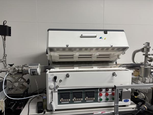 |
| HV CVD-1 (for 2D materials synthesis) | HV CVD-2 (for 2D materials synthesis) | HV CVD-3 (for 2D materials synthesis) |
Characterization Equipments:
 |
Key Features:
|
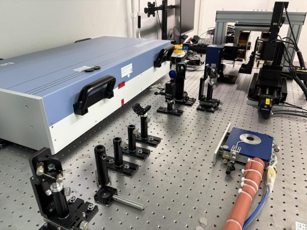
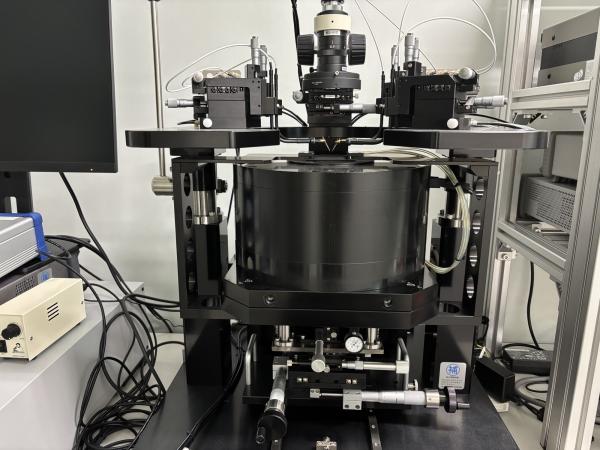
| All-Optical-Switching (AOS) measurement system |
 |
 |
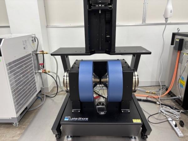 |
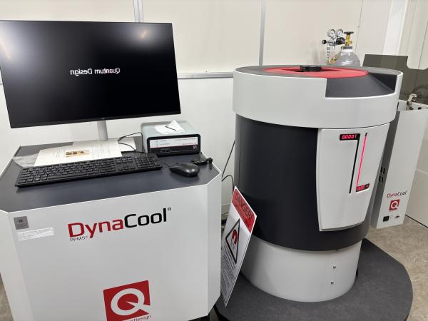
| DynaCool (9T) | MPMS(7T) | VSM (LakeShore8607) |
 |
 |
 |
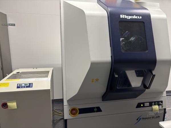
| XRD (SmartLab) | Magnetic prober (perpendicular field max~0.9 T) | Magnetic prober (in-plane field max~0.4 T) |
 |
 |
 |
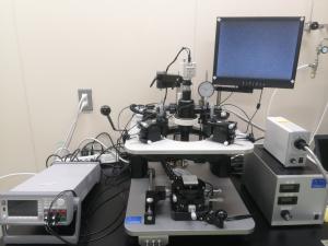
| MOKE (perpendicular field max~1.5 T) | MOKE (in-plane field max~0.1 T) | AFM |
 |
 |
 |
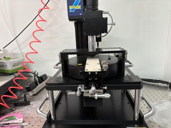
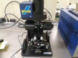
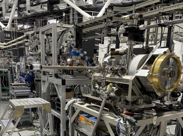
| Raman spectroscopy | XMCD spectroscopy (@BL13U, NanoTerasu) | Mössbauer spectroscopy (@Spring8, BL11XU) |
Micro-fab Equipments:
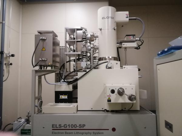 |
Key Features: ・Generates patterns with a minimum line width of 6 nm ・Stable 1.8nm electron beam using high beam current at 100kV ・A 20bit DAC provides high beam positioning resolution ・At a beam current of 1 nA, 20 nm lines can be written over an entire 500μm field without stitching |
| Electron Beam Lithography ELS-G100 |
 |
 |
 |
| UHV magnetron sputter (6 sources) | Ion milling with EPD | Mask aligner |
 |
 |
 |
| Optical microscopy | Wire bonder | Spin coater |