
Home|Research|People|Publication|Facility|Contact|日本語HP
Thin Film Process Equipments:
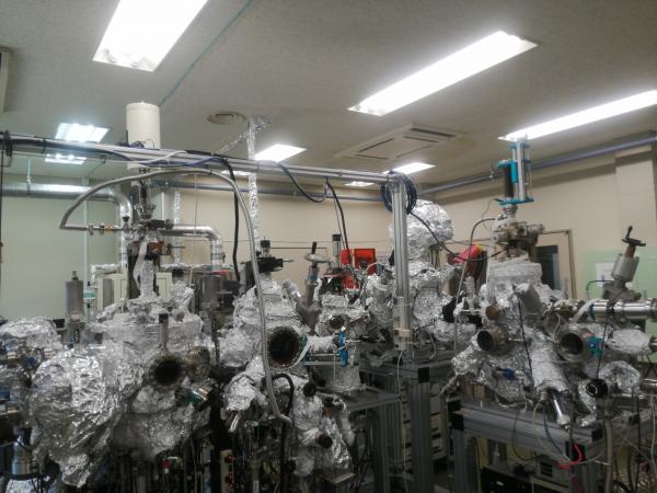 |
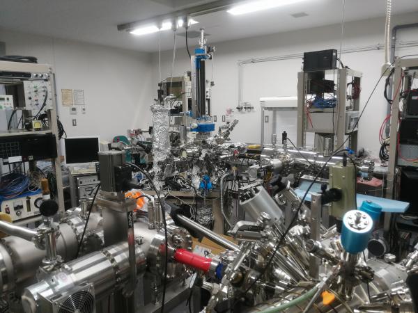
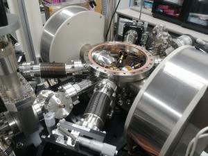
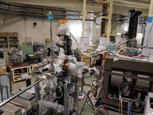
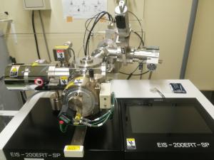
Key Features: ・Transportable through 5 UHV-chambers. ・Deposition function : MBE, Magnetron Sputtering, UHV-CVD, Electron beam deposition ・In-situ Characterization: RHEED, XPS, UPS, EELS |
| UHV multi-function thin film process system |
 |
 |
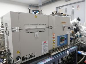 |
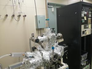
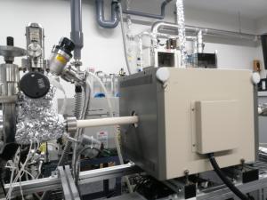
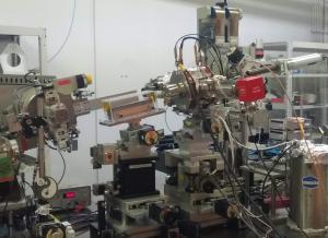
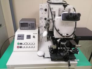
| Magnetron Sputter(RF, 6-gun) | HV CVD-1 | HV CVD-2 |
Characterization Equipments:
 |
Key Features: This system uses a beam of spin-polarized He atoms prepared in the 23S metastable state to probe the spin-split surface density of states (SDOS). When a metastable helium atom is incident on a surface, an Auger-type electron is typically generated through one of two dominant de-excitation mechanisms. The resulting emission electron spectrum contains information only on the SDOS thus making this technique extremely surface sensitive. Measurements can be performed both in-plane and out-of-plane enabling detailed characterisation of the magnetic properties of a variety of surfaces. |
| Spin-Polarized Metastable De-excitation Spectroscopy (SPMDS) |
 |
 |
 |
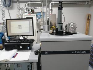
| MPMS(7T) | Raman Spectroscopy | Kerr Microscope |
 |
 |
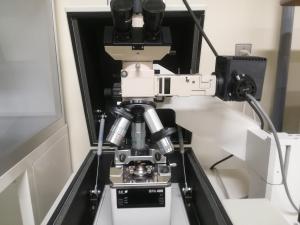 |
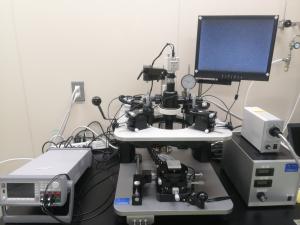
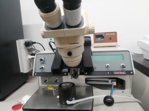
| Low Temp. Prober | Room Temp. Prober | AFM |
 |
 |
 |
| STM | XMCD Spectroscopy (@KEK,PF7A) | Mössbauer Spectroscopy (@Spring8, BL11XU) |
Micro-fab Equipments:
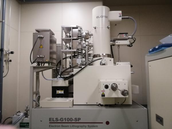 |
Key Features: ・Generates patterns with a minimum line width of 6nm ・Stable 1.8nm electron beam using high beam current at 100kV ・A 20bit DAC provides high beam positioning resolution ・At a beam current of 1nA, 20nm lines can be written over an entire 500μm field without stitching |
| ELIONIX Electron Beam Lithography ELS-G100 |
 |
 |
 |
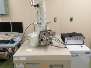
| EBL (JEOL) | Ion milling with EPD | Mask Aligner |
 |
 |
 |
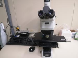
| Optical Microscopy | Wire Bonder | Spin Coater |