Introduction
The Rare-Earth Quantum Device Group is investigating novel quantum devices in which rare-earth (RE) ions are implanted in semiconductors such as nitrides (GaN and AlN) in order to realize the on-chip quantum entanglement light sources and novel quantum sensing. RE ions in GaN can be manipulated as qubits or single photon sources (SPS), which is the building block of quantum technologies.
Development of single photon sources (SPS) and quantum entangled light sources
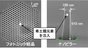
The realization of quantum cryptography and communication, which in principle cannot be eavesdropped or deciphered, requires a technology to generate a single photon on demand. However, there is currently no single photon source in the optical communications band (near-infrared) that can be electrically controlled at room temperature. Neodymium (Nd) and erbium (Er) doped in gallium nitride (GaN) semiconductors show stable near-infrared and narrow linewidth emission even at room temperature, and their photon emission can be electrically controlled (electroluminescence). Therefore, RE ion-doped GaN has a strong potential to be used as an electrically driven SPS. However, the one of the disadvantages is the relatively lower photon emission rates compared to the other SPS candidates (e.g., III-V quantum dots). In order to realize a room temperature, electrically driven, narrow linewidth and near-infrared SPS, we are developing a RE-doped GaN SPS by improving the photon emission rate through optical coupling of implanted RE ions with photonic crystals (PhC) or nanostructures.
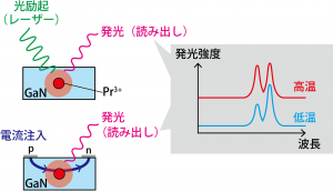
Diagnostics inside nitride semiconductor devices using rare-earth quantum sensors
Quantum sensing is a technique for measuring temperature, magnetic field, electric field, etc. with nanometer resolution using spin resonance and luminescence of point defects and impurities in crystals. In the field of power semiconductors and electronics, the incorporation of quantum sensors into devices is expected to enable real-time measurement of local conditions inside devices and the detection of anomalies and failures. However, currently proposed host materials for quantum sensors are mainly diamond and silicon carbide, and no report has been made on gallium nitride (GaN), which is also a wide-gap semiconductor. We investigate a sensing method using RE ions locally implanted in GaN as a new quantum sensor.